Coating & Surface Testing
Services in India
Validate coating thickness, adhesion rating, microhardness gradients, and corrosion protection layers before putting critical industrial components into service.
When the Surface Layer Is the Component's First Point of Failure
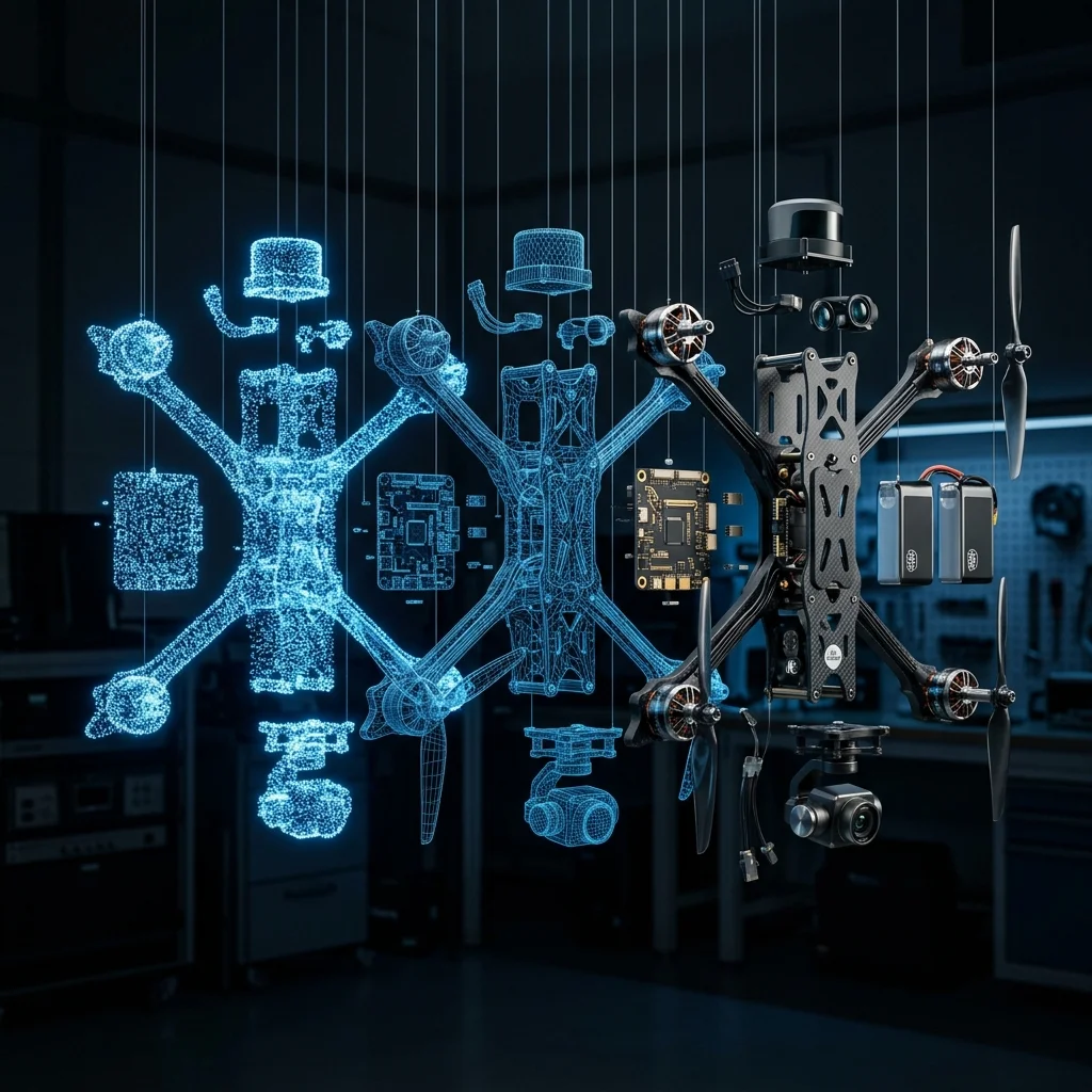
(Scroll or hover to peel back the layers)
Top Finish Integrity
Visual inspection misses micro-porosity and edge build-up issues.
Bond Layer Adhesion
Poor surface prep leads to blistering and delamination under operational stress.
Substrate Impact
Acid treatments induce hydrogen embrittlement in the core metal.
What APJ 3D's Coating & Surface Testing Covers
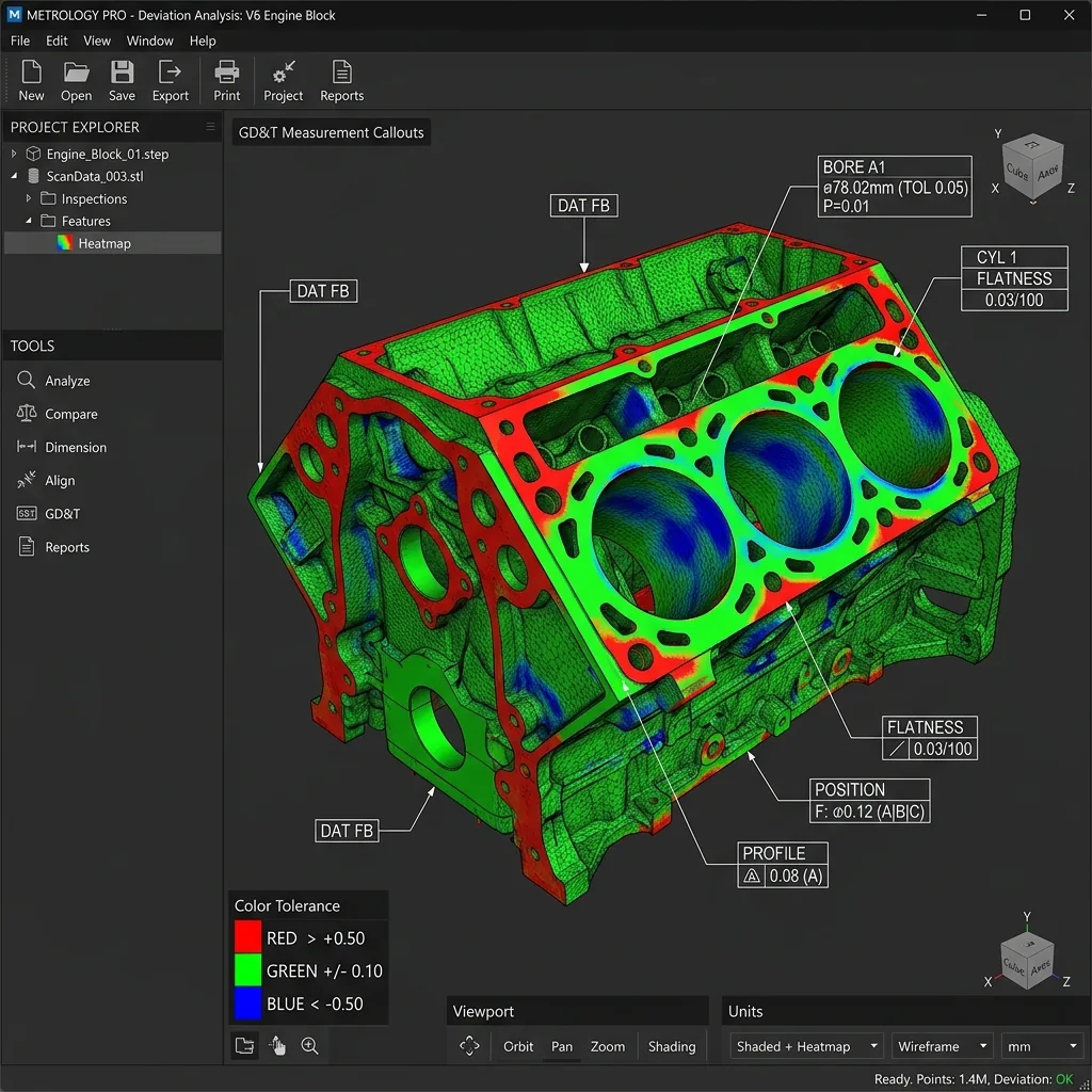
Surface Treatment Testing Service for Industrial Components
Bond Layer
Zinc phosphate or nickel strike. Critical for anchoring the protective coat.
Protective Coating
Primary defense barrier against wear and corrosive environments.
Top Finish
Sealants and chromates providing final operational characteristics.
Different Coatings Require Different Testing Strategies
Electroplating
Zinc, Nickel, Chrome thickness and porosity checks.
Thermal Spray
HVOF cross-section analysis and pull-off adhesion.
Hard Chrome
Microhardness mapping and micro-crack density evaluation.
PVD / CVD
Nano-indentation and ultra-thin film measurement.
Powder Coating
Cross-cut adhesion, flexibility, and impact resistance.
Coating Testing for Automotive Supply Chains
Incoming Verification
PPAP Validation
8D Issue Resolution
Engineering Evidence Delivered
Thickness Mapping
Comprehensive colour thickness distribution map.
Microhardness Profile
Precise hardness transition graphs from surface to core.
Adhesion Test Report
Cross-cut imagery establishing quantitative bond strength.
Surface Integrity QA
Root cause, forensic evidence, and prevention data.
What is Coating & Surface Testing Service India?
3D Scanning is a non-contact optical metrology method that captures millions of precise XYZ surface coordinates using blue light structured fringe projection or handheld laser triangulation, generating high-density polygon point clouds and polygon meshes (.STL, .OBJ).
When to Select This Service
Choose 3D scanning when you need to inspect complex freeform contours, reverse engineer legacy components without CAD blueprints, analyze casting wall thickness, or align sheet metal stampings against master CAD models.
Technical Capabilities & Verification Standards
Verified engineering parameters, hardware precision, and compliance benchmarks applied across all deliverables.
| Engineering Parameter | APJ 3D Capability & Precision Range | Compliance Standard / Verification |
|---|---|---|
| Coating Thickness Measurement | Eddy-current thickness measurement of coating layers on industrial components | ASTM B499 / ISO 2178 |
| Adhesion Testing | Cross-cut adhesion rating to verify bond strength between coating and substrate | ASTM D3359 Cross-Cut Adhesion |
| Microhardness Profiling | Microhardness mapping and micro-crack density evaluation across coating cross-sections | ASTM E384 Microhardness |
| Coating Types Covered | Electroplating, HVOF thermal spray, and powder coating cross-section and adhesion analysis | Multi-Process Coating Coverage |
| Corrosion Protection Validation | Verification of corrosion protection layers before critical industrial components enter service | Pre-Service Protection Validation |
| Laboratory Verification | Independent laboratory verification of supplier coating batches | Independent Batch Verification |
Frequently Asked Questions
Can you perform 3D scanning on-site at our manufacturing plant?
Can you perform 3D scanning on-site at our manufacturing plant?
How do 3D scanning and reverse engineering differ?
How do 3D scanning and reverse engineering differ?
What is a color deviation inspection map?
What is a color deviation inspection map?
Can dark, shiny, or transparent surfaces be scanned?
Can dark, shiny, or transparent surfaces be scanned?
What accuracy can we expect for automotive and aerospace components?
What accuracy can we expect for automotive and aerospace components?
Verify Coating Thickness & Adhesion Before
Production Makes the Decision Permanent.
Leverage our reliable eddy-current thickness measurement, cross-cut adhesion, and microhardness testing services in India. Secure your supplier batches with independent laboratory verification.